


Whitepaper Download
Know more, achieve more
Technical whitepapers for engineers
Of the many ways to join components in manufacturing, adhesive bonding is a more sophisticated method. A solid understanding of its basic principles and special aspects is essential to meet its complex requirements.
Get free groundbreaking whitepapers that provide insights into how you can optimize and improve your adhesive bonding processes. Take advantage of our expert knowledge and benefit from these insights.
What awaits you…
- Detailed functionalities of the processes
- Necessary requirements
- Suitable materials for the respective application
- Possible areas of application
- Novel perspectives in product design
- …and much more!
Whitepaper
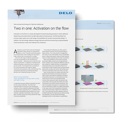
2-in-1 bonding:
Activation on the Flow
Industrial mass production requires fast and efficient processes, which can reduce costs and help companies reduce their carbon footprint. Learn how one of our newest technologies, Activation on the Flow, can help you implement these processes in this eponymous whitepaper.
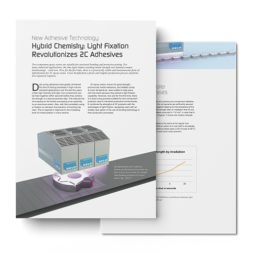
Fixing two-component epoxy resins under UV light
In this free whitepaper, you will learn how adhesive strength can also prove itself under the influence of temperature and humidity. In addition, find out how innovative technology makes transportation and storage more efficient and less expensive.

Thermally conductive adhesives for low-voltage battery cells
Thermally conductive adhesives bond low-voltage battery cells to housings, providing thermal management for efficient heat dissipation. Learn how this application eliminates the need for spacers or thermal pads, saves process steps and simplifies production operations.
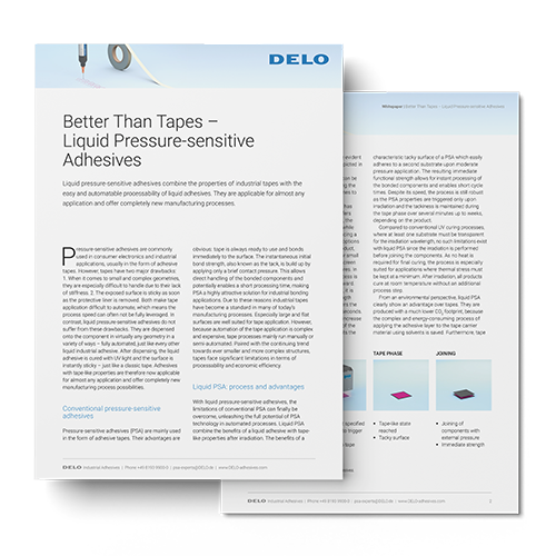
Better than tape: Pressure-sensitive adhesives
This innovative solution combines the advantages of light curing with the qualities of 2C products. Soon, facilities will only require one mixing and lamp system. This leads to savings in energy, time, and space. Learn more in this white paper!
Full-wafer double-sided
monolithic lens fabrication
Monolithic lens array production without glass substrates is steadily rising. This new method of production increases the scalability and material compatibility of optical devices, which then brings higher efficiency and cost-effectiveness. This whitepaper goes over SUSS UV imprint lithography with tailored, UV-curable epoxy resins for double-sided wafer-level optics.
Nanoimprinting UV-curable
polymers on 300 mm wafers
Together with experts from Germanlitho, DELO has been researching wafer-level manufactured nanostructures. Their findings show exciting possibilities for making augmented reality suitable for mass production using solvent-free adhesives.
UV lens molding for
wafer-level micro-optics
Refractive polymer microlenses are central to the construction of micro-optical modules. Methods of wafer-level UV lens forming, especially nanoimprint lithography and lens molding, work with complex structures, thus suitable for a wide variety of applications.
In this whitepaper, EVG and DELO present an industrial solution that allows you to combine processes and materials for high-quality lenses with pattern fidelity.