Thanks to micro- and nano-optics, ever more compact optical systems are being created. These pave the way for completely new functionalities that cannot be achieved with conventional optics. UV imprint, meanwhile, makes the cost-efficient mass production of such optics has become a reality. However, if additional functions, such as electrical conductors or black apertures, are to be integrated into the optical module, complex processes (e.g., photolithography) are often used. These processes are not only expensive, but also not ideal when combined with the UV imprint process. By combining different functional polymers, you can reduce costs, simplify the process and increase the reliability of the optical element.
What are micro-optics and where are they used?
Put simply, micro-optics are miniaturized versions of conventional optics. Components of the latter, such as lenses, mirrors or prisms, are only a few orders of magnitude longer than the wavelength of light passing through them.
Medical endoscopes are one application where the advantages of reducing the size of optics become particularly clear. In recent years, micro-optics and corresponding manufacturing techniques have enabled the entire optical module (including the image sensor) to be reduced to a cube with an edge length of <1 mm (see Figure 1a).
In addition to the smaller dimensions, micro-optics also enable new and improved concepts for centuries-old optical tasks, such as projection systems. Instead of using individual lenses arranged one behind the other to create a bulky setup for image projection, an array of microlenses is used to parallelize the projection. This achieves a high luminous flux at a fraction of the size of conventional projection systems thanks to a shortened focal length (see Figure 1b).
If the dimension is reduced from micro- to nanoscopic, this changes the light steering method from refractive to diffractive. This opens up a wealth of new possibilities. For example, diffractive optical elements (DOEs) can be used to change a collimated (straight) laser beam into virtually any desired light distribution. A notable example is the creation of a dot pattern used in 3D sensing to measure the width, height, and depth of an object (see Figure 1c).
How does the manufacturing process work?
This new type of optic naturally requires new manufacturing methods. Conventional methods, such as injection molding, are less suitable due to their required structure sizes and precise alignment.
The UV micro/nano-imprint process is now an established tool readily available on standard machines offered by several manufacturers. Here, a liquid, transparent UV-curing material is applied to a glass wafer, then brought into contact with a structured stamp. Once the geometry of the optics, such as lenses and DOEs, has been defined by the stamp, the material is cured by UV light. The stamp is then removed, and the structured wafer is cut into individual modules (see Figure 2).
Integration of apertures as a functional layer
Things get slightly more complicated when additional features need to be integrated into an optical element. Apertures, for example, are key elements in many optical designs.
Until now, apertures have been integrated into imprinted optics as standard using a photolithographic process. This involves first creating a structured chromium layer on a glass wafer and then imprinting the optics directly onto the wafer.
The photolithographic process involves a large number of steps:
- Coating a glass wafer with a homogeneous chromium layer
- Depositing a photoresist
- Structuring of the photoresist using a lithography step
- Chemically developing of the photoresist
- Removing part of the chromium layer
- Removing the remaining photoresist
Disadvantages of this solution:
- This process is very complex and, therefore, expensive.
- It also severely restricts the possible applications for such apertures. This process only works on glass wafers and is generally not compatible with the structuring of a chromium layer on the polymer optics themselves.
- Further problems can arise due to insufficient adhesion of the chromium layer to glass or of the polymer material to chromium.
New approach 1: Direct embedding of a functional material in the optics
Many of the aforementioned problems can be avoided by embedding a functional (e.g., black) material directly into the polymer optics. One way to achieve this is to imprint defined channel structures in addition to the optical structure during the imprint process. These channels can then be filled with a black, low-viscosity material that is cured either by UV light or heat (see Figure 3). This simplifies the process enormously.
Another advantage of this option is that the thermomechanical properties of the two materials (optically transparent and black) are much closer to each other than those of glass, chromium and polymer. This avoids thermal stresses caused by mismatches in the coefficient of thermal expansion (CTE). This directly improves reliability, as temperature cycling tests have shown. As this method no longer requires glass substrates, the weight and height of the optics are effectively minimized, and costs are reduced at the same time.
New approach 2: Use of a temporary carrier
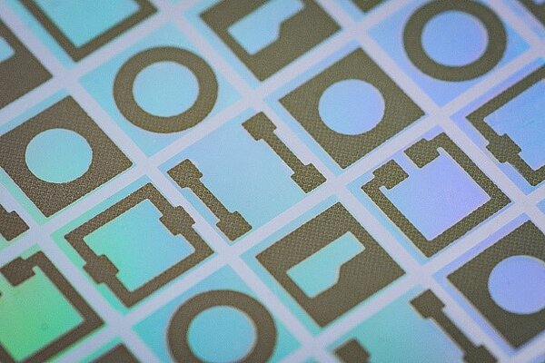
Another possible approach is to start with a temporary carrier (e.g., a plastic foil). The apertures are produced on the carrier by screen printing a light-blocking polymer. After UV or heat curing the polymer, the standard UV imprint follows, where the optical structures can be precisely aligned with the apertures. Once the transparent material has cured and the stamp has been removed, the carrier foil can be peeled off. The result is a completely monolithic (all-polymeric) optical module with integrated apertures (see Figure 4).
Both new approaches have the common advantage in that the properties of black materials can be adapted to either optical design and its respective processes:
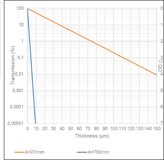
- Example 1: A screen-printable material with moderate viscosity and a high absorption coefficient for high optical density in a few µm thin layers.
- Example 2: A material for filling functional structures with low viscosity and a moderate absorption coefficient for high optical density in structures of a few 100 µm.
- It is even possible to incorporate a spectral filter function directly into the polymer (e.g. blocking a certain wavelength range while allowing transmission in another wavelength range).
Integration of functional, electrically conductive layers
Some applications require the integration of electrically conductive structures into the optical element. One example is the diffuser element used in time-of-flight sensors or for structured light sensors that form the collimated laser beam of the emitter. Here, the conductive structures are used as a safety net to detect possible damage to the diffuser element, thus avoiding any threat from the emitted laser beam. A process similar to that used for the apertures can be used to produce such a safety net. However, an isotropic electrically conductive adhesive (ICA) is used instead of a black polymer.
First, an ICA (e.g. DELO DUALBOND IC343) is screen-printed onto a temporary carrier foil containing various structures (e.g. conductor tracks, apertures). A transparent, UV-curing material (e.g. DELO KATIOBOND OM614) is then used to print a nanostructure onto this foil, which forms the diffractive optical element. Peeling off the carrier foil creates a full polymer wafer with several DOEs and an integrated conductive structure (see Figure 6).
Conclusion
This process impresses with its simplicity and cost efficiency:
- Simple UV imprint processes can be used to produce miniaturized optical elements such as lenses or DOEs with additional functionalities (e.g. electrical conductors or black apertures).
- Only two materials are required for this: A UV-curing transparent material for the main optics and a UV- or heat-curing filled material that provides the electrical conductivity or light-shielding property.
- This approach also makes it possible to overcome potential reliability problems (e.g. thermal mismatch), as the thermomechanical properties of the two materials can be matched.
At DELO you will find an extensive portfolio of such products. We will help you to find a suitable solution for the specific requirements of your individual application.


